











-
VCSEL Chips

VCSEL Core Technologies and Innovations
Raysees VCSEL technology is not built on imitation, but on original innovation. We focus on solving the core bottlenecks of VCSELs in optical sensing — performance, mass production, and application integration — driving continuous breakthroughs from chip design to system deployment.
-

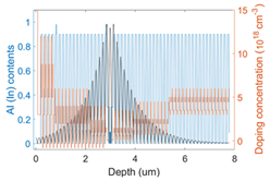
Epitaxial Design
-
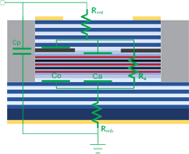
Device Design
-
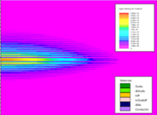
Electromagnetic Simulation
-
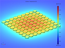
Thermal Management
Solving Key Challenges
-
How can VCSELs break performance limits for advanced optical applications?
-
How do we simplify optical system integration while maximizing VCSEL system performance?
-
How can VCSELs deliver higher performance for complex optical applications?
Highlights
-

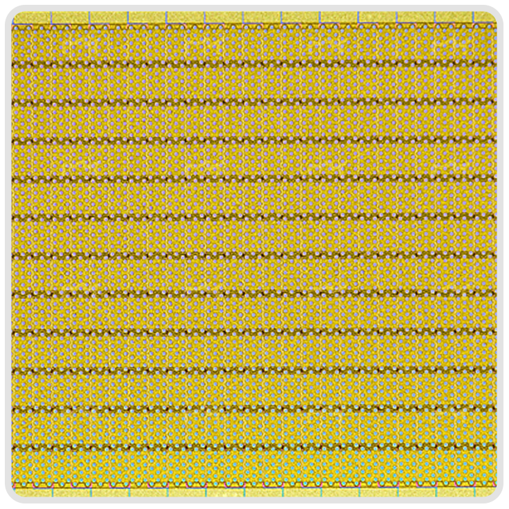
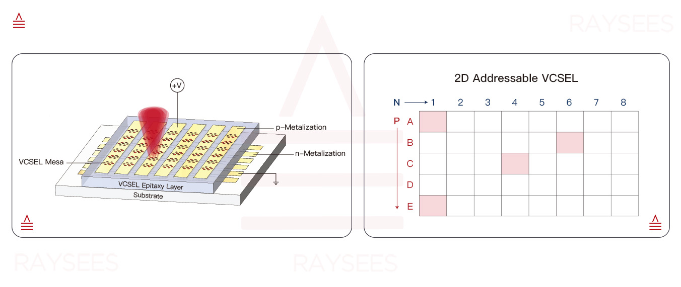
Automotive 2D Addressable VCSEL
Pixel-level control
for robust LiDAR -
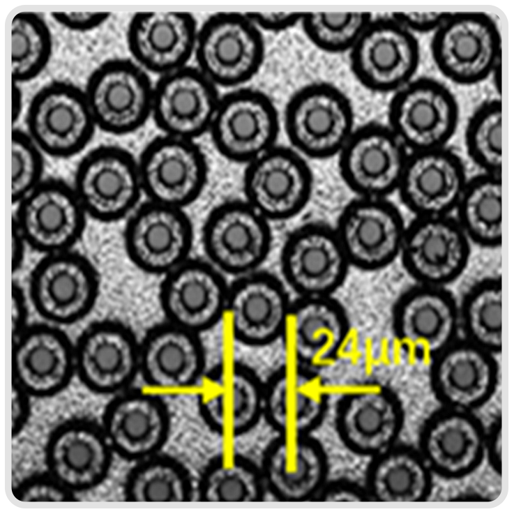
High-Density Random Array
<24 µm pitch
higher density -
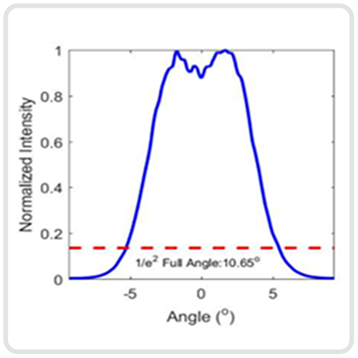
Oxide-Confined Narrow-Divergence VCSEL
<15° divergence for
compact optics. -
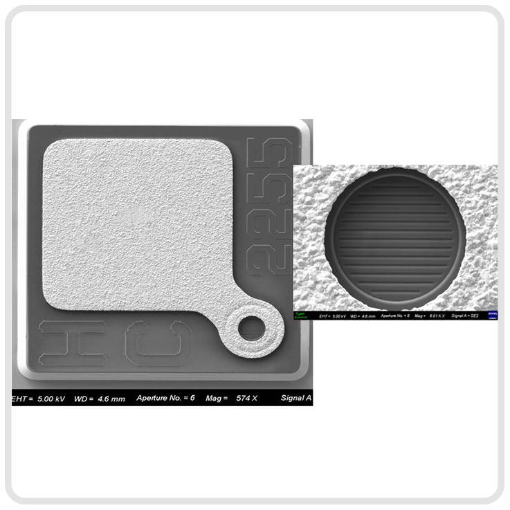
Single-Mode Polarized VCSEL
Stable polarization
high-SNR sensing -
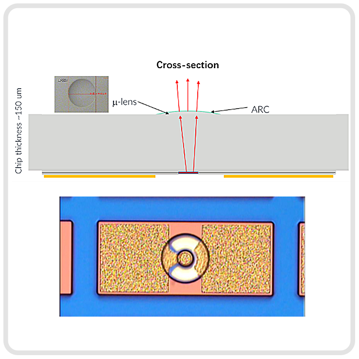
Flip-Chip VCSEL
Microlens integration
for beam shaping -
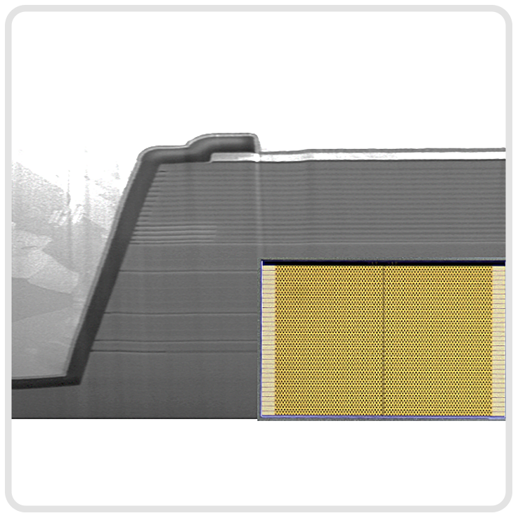
Multi-Junction VCSEL
High optical density
for compact devices -
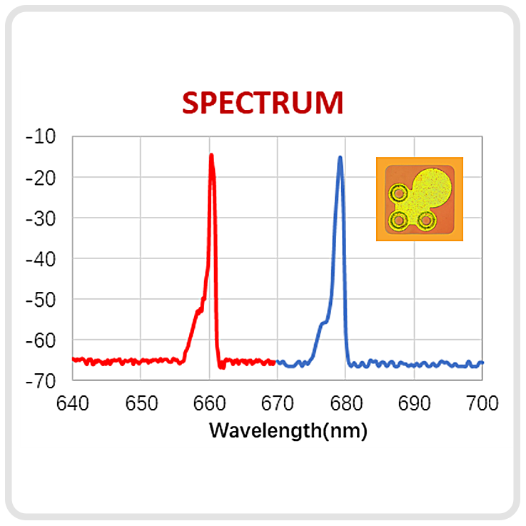
Red VCSEL
Visible emission for
health sensing -
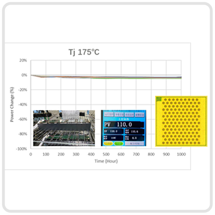
Automotive CW VCSEL
Validated CW reliability
for automotive systems
Core VCSEL Technologies
Solving industry bottlenecks through proprietary chip innovation
-
01 2D Addressable VCSEL
-
02 Ultra-Low-Divergence VCSEL
-
03 Backside-Emitting Microlens VCSEL
-
04 High Power Density & High Peak Power VCSEL
-
05 High-Speed Datacom VCSEL
Raysees 2D Addressable VCSEL enables pixel-level electrical addressing at the chip level. Built on a highly uniform vertical-cavity resonant architecture, it supports selective pixel activation, dynamic pattern projection, and programmable timing control — delivering higher optical power density and greater system flexibility for intelligent LiDAR sensing.
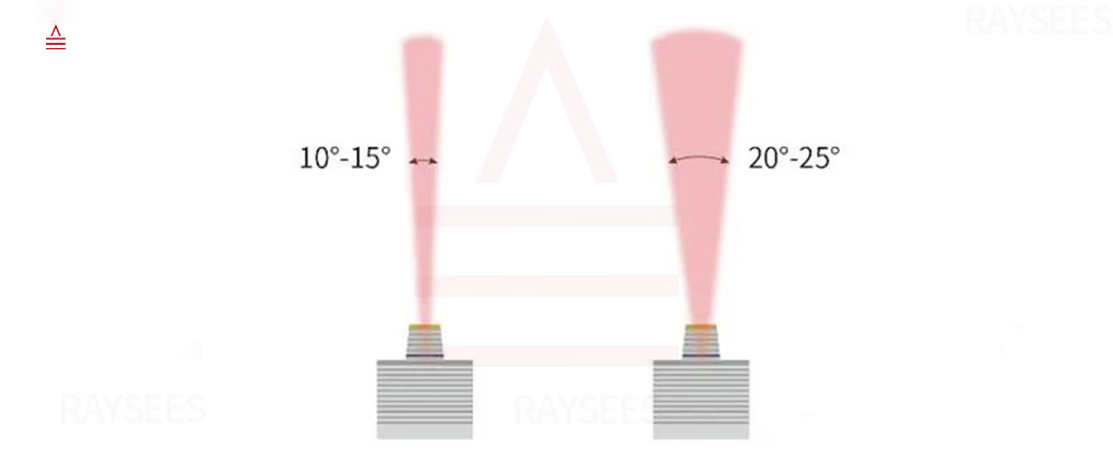
Raysees Ultra-Low-Divergence VCSEL technology uses advanced chip architecture and process optimization to achieve <15° beam divergence while maintaining high optical output power. It reduces optical crosstalk between the transmit and return paths, enabling more compact proximity sensing modules, simplified optical design, and higher-precision distance measurement.
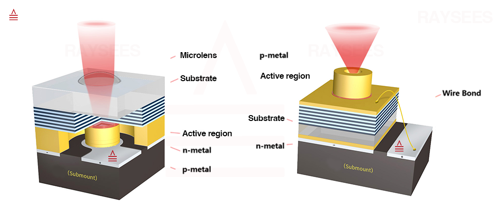
Raysees backside-emitting microlens-integrated VCSEL uses a flip-chip architecture for faster pulse rise/fall times and higher peak optical power. By integrating microlenses on the backside-emitting VCSEL, it improves beam control while reducing optical stack height — enabling compact sensing modules for space-constrained smartphones, VR, and AR systems.
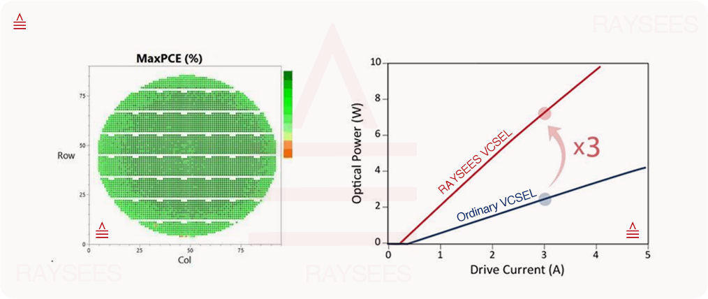
Raysees high-power-density, high-peak-power VCSEL technology delivers several times higher optical output power without increasing chip size, while improving power conversion efficiency. It enables compact, long-range optical sensing systems for applications such as 3D dToF and LiDAR.
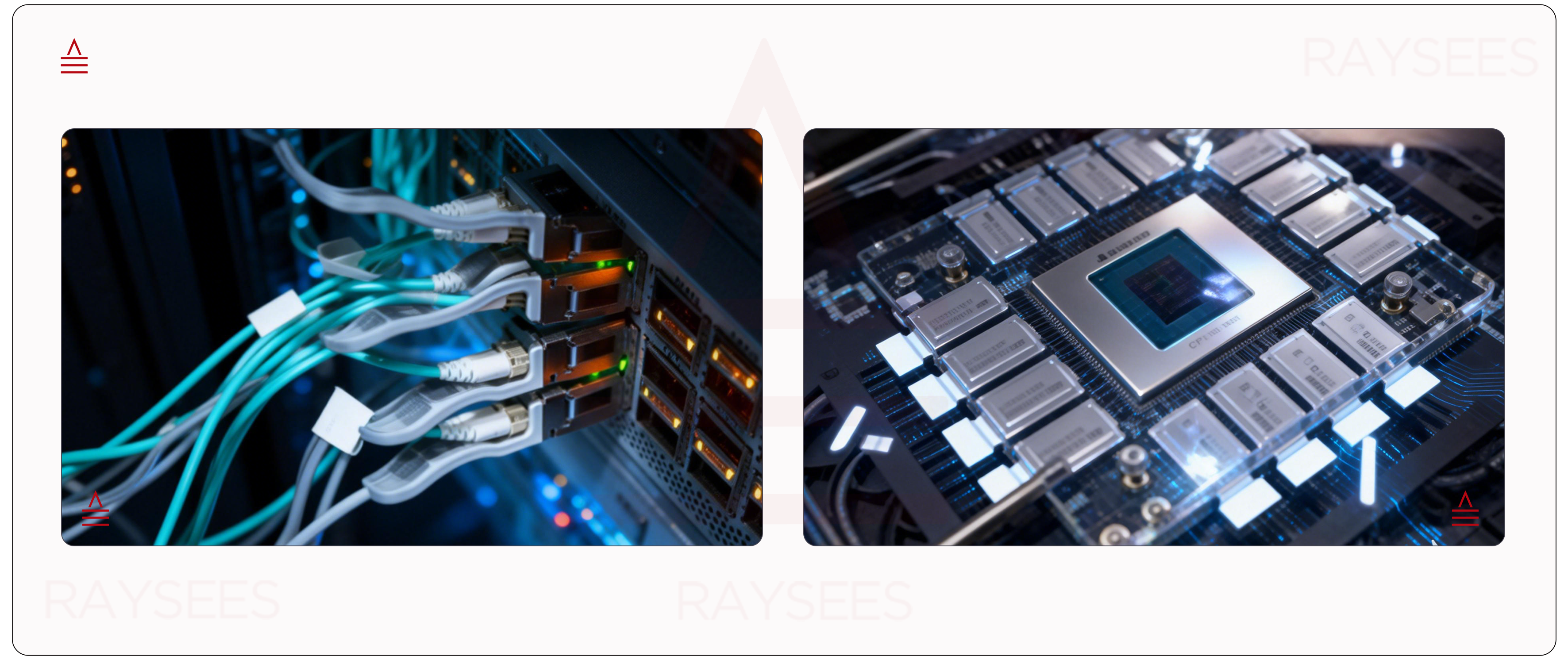
High-speed VCSELs serve as core light sources for short-reach interconnects in data centers and AI clusters, primarily in parallel optical links. Optimized for array uniformity, modulation performance, and long-term reliability, they enable scalable bandwidth, controlled power consumption, and stable operation for next-generation optical modules.

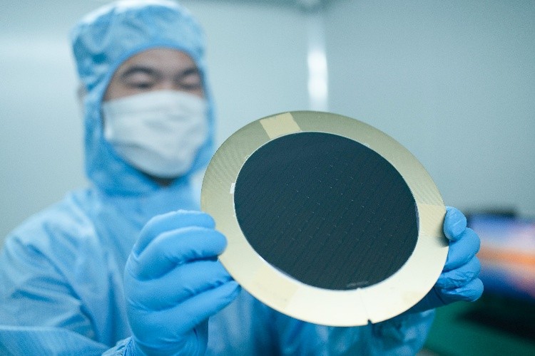

Scalable VCSEL Manufacturing
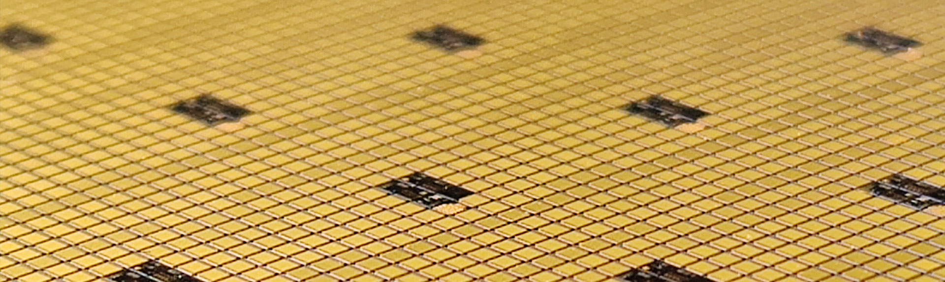
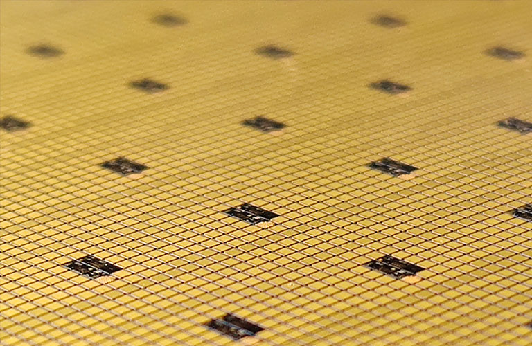
Raysees delivers high-quality VCSEL chips at scale, with optimized process control, proven reliability, and stable wafer-level yield above 90%. With over 200 million chips shipped, Raysees has built a mature volume manufacturing platform supported by world-class epitaxy and wafer foundry partners.